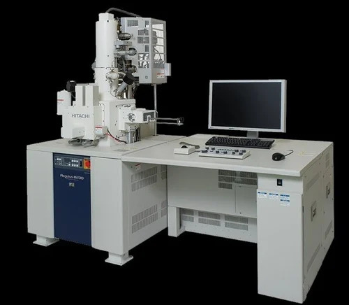
About Scanning Electron Microscope
The Scanning Electron Microscope-Highly Recommended for advanced imaging-blends phenomenal resolution with venerable reliability. Its glorious 3 nm resolution at 30 kV, versatile emission source options (Tungsten filament or field emission gun), and proprietary digital imaging sensor deliver unmatched clarity. Equipped with a robust, oil-free vacuum system and chamber delivering up to 300 mm diameter compatibility, it handles large specimens effortlessly. Multi-modal detection, advanced specimen handling, environmental controls, and seamless software integration ensure comprehensive analysis. Shop Now to experience scientific excellence and unlock a new standard in microscopic imaging!
Application Media, Competitive Edge & User Base
The Scanning Electron Microscope is invaluable in research labs, industry, material science, biology, and forensic analysis-offering users exceptional imaging and analytical capabilities. Its competitive advantages include phenomenal multi-detector support, high-resolution imaging, and automated analysis tools. Used by top manufacturers, universities, quality assurance teams, and scientific research institutions, it ensures superior insights across application media, giving users a remarkable edge in discovery and innovation.
Domestic Market Reach, Port & Sample Exchange Value
With prompt arrival in the main domestic market across India, this SEM holds outstanding market value for professionals and institutions alike. Shipped from a reputable FOB Port, it comes with sample availability for evaluation and exchange, ensuring user satisfaction and investment confidence. This instrument's capabilities and support structure make it a preferred choice, elevating user experience and strengthening its position in the competitive microscopy market.
FAQ's of Scanning Electron Microscope:
Q: How does the Scanning Electron Microscope achieve such high resolution?
A: The SEM achieves up to 3 nm resolution at 30 kV using a precisely focused beam of high-energy electrons, advanced emission sources, and state-of-the-art digital imaging sensors. Its multi-detector arrangement enhances imaging clarity and detail for various specimen types.
Q: What advantages does this SEM offer compared to traditional light microscopes?
A: This SEM allows for magnifications up to 300,000x with superior depth of field, providing highly detailed, three-dimensional surface information, which is far beyond the capabilities of traditional optical technologies.
Q: Where can I use this SEM and who typically benefits from it?
A: This SEM is widely used across universities, research centers, manufacturing quality control, materials science, biology, and forensic analysis, benefiting scientists, engineers, and lab professionals seeking in-depth specimen analysis.
Q: What is the process for specimen preparation and imaging?
A: Specimens are mounted on compatible stubs, placed in the spacious chamber, and imaged under vacuum, using adjustable emission voltage and multi-axis motorized staging for precise observation. Automated software aids in capturing and analyzing images efficiently.
Q: Is a sample unit available for evaluation before purchase?
A: Yes, sample units are available for assessment upon request, allowing potential users to evaluate features and performance, ensuring it fits application requirements before committing to full-scale acquisition.
 Send Inquiry


 Send Inquiry
 English
 Spanish
 French
 German
 Italian
 Chinese (Simplified)
 Japanese
 Korean
 Arabic
 Portuguese